
Plasma
Plasma
In the semiconductor industry, plasma processes are widely used for both atmospheric decapsulation and vacuum cleaning applications.
Atmospheric plasma decapsulation is a technique designed to remove encapsulating materials, such as epoxy molding compounds, from integrated circuits without damaging the silicon die. This process typically uses a reactive plasma generated at atmospheric pressure, eliminating the need for vacuum chambers. Reactive species, such as oxygen radicals and ions, chemically break down organic materials into volatile byproducts that can be safely extracted. Because it operates at atmospheric pressure, the system can be more flexible and cost-effective.
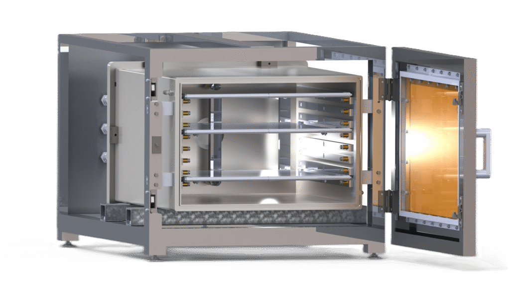
Vacuum plasma cleaning, on the other hand, takes place inside a controlled low-pressure chamber. In this environment, gas molecules are ionized by an electric field, creating a stable and uniform plasma. The reduced pressure increases the mean free path of particles, enhancing reaction efficiency and surface uniformity. Plasma cleaning under vacuum is highly effective for removing organic contaminants, thin oxide layers, and residual photoresist from wafer surfaces. It also improves surface energy, promoting better adhesion for subsequent processes such as wire bonding, die attach, or thin-film deposition.
Both atmospheric decapsulation and vacuum plasma cleaning rely on the interaction between energetic ions, radicals, and the material surface. These techniques provide precise, controllable, and non-contact material removal, making them essential tools in advanced semiconductor manufacturing and failure analysis.
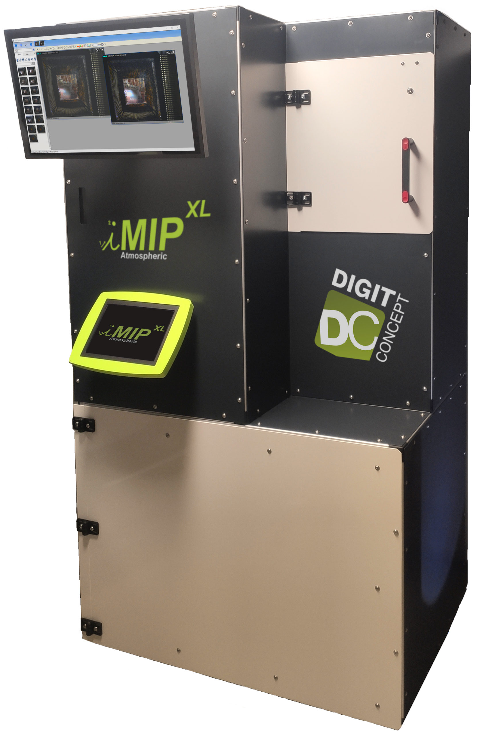
First and only qualified system to interface with patented decapsulation technology in atmosphere plasma.
All types of Plasma Cleaning Tools Cleaning Surface Activation Stripping Photoresist Cleaning…